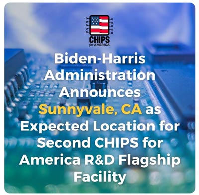
November 4, 2024 - WASHINGTON, D.C. — Last Friday, U.S. Senator Alex Padilla (D-Calif.) issued the following statement after the 
Related: California Governor Gavin Newsom Announces San Francisco Bay Area Selected as National Semiconductor Technology Center Headquarters
The DCF in Sunnyvale, California, will be a colocation of the NSTC headquarters and the flagship design hub from where all NSTC R&D work will be coordinated. The headquarters will serve as a site to host NSTC member and semiconductor ecosystem convenings, NSTC programmatic activities, the Workforce Center of Excellence, the future investment fund, and more. The national design facility will include the NSTC Design Enablement Gateway and an institution for design research focused on chip design, electronic design automation, hardware security, and chip system architecture.
“California is the clear choice to lead NSTC’s semiconductor innovation and R&D. Our state has built a world-class innovation economy and has been at the forefront of the semiconductor industry for decades. We are uniquely positioned to leverage our R&D, manufacturing capacity, and end-users to drive this industry forward.
“Establishing the NSTC headquarters in California will capitalize on our state’s unparalleled assets to grow a highly skilled workforce and develop next-generation advancements. I am confident that this CHIPS Act funding will propel emerging technologies and protect America’s global semiconductor leadership, all while bringing good-paying jobs to our state.”
Santa Clara County alone holds 20 percent of all semiconductor utility patents granted in the last decade, and California is home to more semiconductor R&D, design, intellectual property (IP), and electronic design automation (EDA) firms than Texas, New York, and Oregon combined – with over 175 companies operating out of Silicon Valley. The design facility is one of three planned major NSTC centers. The Department of Commerce recently announced the Extreme Ultraviolet (EUV) Accelerator in New York, and said a Prototyping and NAPMP Advanced Packaging Piloting Facility is still forthcoming.
In April, Padilla, Senator Laphonza Butler (D-Calif.), Representative Zoe Lofgren (D-Calif.-18), and Representative Doris Matsui (D-Calif.-07) led the entire California Democratic delegation in urging Secretary of Commerce Gina Raimondo to establish the NSTC headquarters in California. The letter came after Padilla and Governor Gavin Newsom issued a statement rebuking the CHIPS Program Office’s (CPO) cancellation of the third CHIPS Act Notice of Funding Opportunity (NOFO) for advanced commercial research and development facilities in the United States.
In 2022, Senator Padilla and Senator Reverend Raphael Warnock (D-Ga.) sent a letter urging Senate leadership to support provisions in the final version of the United States Innovation and Competition Act that would require semiconductor companies receiving federal assistance for research, design, and manufacturing to invest in a more diverse workforce and improve procurement from minority-, veteran-, and women-owned businesses. Padilla and Warnock applauded the passage of one of these provisions through the Creating Helpful Incentives to Produce Semiconductors (CHIPS) for America Act later that year.
Source: Senator Alex Padilla


